U.S. Department of Transportation
Federal Highway Administration
1200 New Jersey Avenue, SE
Washington, DC 20590
202-366-4000
Federal Highway Administration Research and Technology
Coordinating, Developing, and Delivering Highway Transportation Innovations
 |
| This report is an archived publication and may contain dated technical, contact, and link information |
|
Publication Number: FHWA-RD-02-034
Date: September 2005 |
||||||||||||||||||||||||||||||||||||||||||||||||||||||||||||||||||||||||||||||||||||||||||||||||||||||||||||||||||||||||||||||||||||||||||||||||||||||||||||||||||||||||||||||||||||||||||||||||||||||||||||||||||||||||||||||||||||||||||||
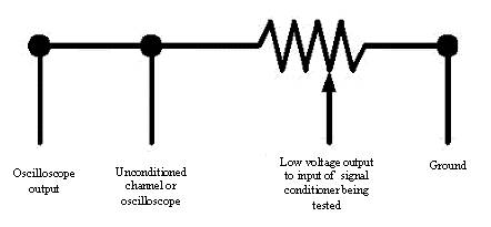
Long-Term Pavement Performance Materials Characterization Program: Verification of Dynamic Test Systems With An Emphasis On Resilient ModulusChapter 3. ELECTRONIC SYSTEMS PERFORMANCE VERIFICATION PROCEDUREINTRODUCTIONBased on multiple system evaluations, it has been found that the electronics verification procedure is by far the most complex and difficult portion of the evaluation procedure. Because of the inherent complexity of this task, this section of the document provides an expanded discussion of the theory and rationale behind the procedure. Many different types of test systems are on the market today. Generally, each of these systems contains its own vendor-proprietary method for signal conditioning. Because of the wide variety of system configurations, this section of the document has been developed to present the general approaches to electronics evaluation. Users are advised to select the most applicable method for their system and apply the concepts presented here to characterize and verify the system. It is strongly recommended that personnel with a background in electronics and mechanical systems perform these procedures. Performance of these procedures by unsuitably qualified personnel may result in system damage, physical injury, or other undesirable consequences. The entire system—software, data-acquisition system, control electronics, hydraulics, and mechanical aspects of the test system—needs to be operating in a controlled and safe manner before the verification procedure can be completed successfully. BACKGROUNDWhen performing a test, it is generally accepted that the test transducers be calibrated. In this procedure, the output of the transducer is compared to a known test value (e.g., a load, pressure, or displacement), and a relationship (usually linear) is developed between the transducer output and the known applied test values. The resulting curve is the transducer calibration. This calibration procedure is a required element if the user is to know the test values being applied to a sample under test. But this calibration is by no means the only factor that influences the test readings. The calibration procedure may not account for the system electronics, and it certainly does not account for time-varying test conditions. If the test system electronics are improperly configured, the test readings may be quite wrong, even if the transducers are calibrated. The purpose of this verification procedure is to assess the dynamic system performance of the data-acquisition system (DAS) so that the user is confident that the values measured by the computer are in fact the loads, displacements, and pressures being applied to the sample. To perform this verification test on the DAS, known signals (known in time and magnitude) are applied to each conditioned channel in succession, and the response of each channel is compared to the known applied signal. These verification tests are performed “in-system” to as great an extent as possible so that the entire transducer/conditioning/acquisition system is incorporated in the verification test. An additional benefit of performing these verification tests is that the test system is exercised and the operators become more familiar with both system software and hardware. If an open mind is used to analyze the sources of error and aberrations that are exhibited during these tests, then other interrelated shortcomings of the system can often be deduced and rectified, resulting in a more robust and properly operating system. Therefore, the procedure should not be used in a cookbook manner. Instead, the objective of each task and the response of the system should also be understood, rather than applying a “go/no-go” mentality. An attempt has been made to compartmentalize the various tasks of the verification procedure, but as the user works with the system, the user realizes that each component contributes to the proper functioning of the whole system. The interactions between the system components sometimes make it difficult to troubleshoot a system without understanding all of the subcomponents and the interactions among these subcomponents. This procedure has been developed to evaluate the filter settings of the signal conditioners. When a signal passes through a filter, the signal is delayed by a constant amount (the delay of which is for the most part independent of the frequencies used in these tests). In addition, the signal is attenuated as the signal frequency increases past the cutoff frequency of the filter. If the input to the conditioner is compared to the output signal over a range of frequencies, the user can identify the type of filter and the cutoff frequency of the filter. More important, the user can evaluate whether the conditioned signal closely duplicates (both in magnitude and in time) the physical processes being monitored. The procedure used to evaluate the filter settings was initially developed using a wholly electrical approach in which the transducers were electrically simulated. This approach works well for direct current (DC) type signal conditioners, but has serious drawbacks for transducers that rely on alternating current (AC) excitation (e.g., LVDTs). For these AC-excited transducers, a new simulation interface circuit has to be designed, built, and tested for each type of AC signal conditioner. The new construction and testing of the test circuit is in itself a task that is quite labor intensive, and the final test circuit could introduce noise. In addition, any errors introduced by the circuit need to be quantified. Another issue with this approach is that the new circuit needs to be tested in the system before it is deemed acceptable. This approach is very time consuming. To work around these shortcomings, a mechanical approach was developed to actuate the system LVDTs and test the AC conditioning system by comparing the movement of a reference LVDT to the displacement of the system LVDT being tested. (This mechanical LVDT actuator could be further modified to include a strain-gauged member that would be mechanically flexed and result in a Wheatstone bridge output that could be used to simulate a load cell. Thus, with this mechanical actuator, no electrical simulations would be required to perform the verification tests.) An alternative procedure to the electrical simulation has been developed for evaluating the load cell channels. In this approach, the load cell is physically actuated using the hydraulic loading system. The hydraulic loading ram applies a sinusoidal load at frequencies up to 50 hertz (Hz). Generally, most systems encountered to date seem to be limited to a frequency of about 20 Hz (although this may be software limited rather than being limited by the hardware). Due to this inability to reach 50 Hz, the DC conditioners will have to be electrically simulated unless this limitation can be overcome. A note concerning filter settings is warranted: Low-pass filters are an integral part of most signal-conditioning systems. They are used to smooth out the desired signals and to block high-frequency noise that may be superimposed on the desired signal. In the case of AC conditioning systems, they also filter out any residual noise resulting from the carrier frequency. With such benefits to be gained from filters, it is tempting to add as much filtering as possible. The problem with this approach is that the filters also introduce a time delay and tend to attenuate the desired signal as the frequency of the designed signal starts to approach the cutoff frequency of the filter. It is best to set these low-pass filters as high as possible and yet still obtain a smooth signal. These filter settings should be recorded and tests performed with these filter settings. Before settling on these filter settings, the user should operate the test system under various conditions, for various periods of time, and at various times of day to ascertain the settings when a variety of operating environments are encountered. Starting and stopping of large inductive motors creates a particularly large amount of electrical interference. To account for these potential sources of electrical noise, air conditioners, compressors, hydraulic pumps, and other large motors should be started and stopped when taking data in an attempt to identify sources of noise that might impact the system. Filter cutoff frequencies should be set to reduce this noise to a tolerable level. If reducing the filter settings does not reduce the noise sufficiently, the test system should be isolated from the source of the electrical noise. Typically, a test system uses filters of the same type on each of its channels. In this instance, it might be a good policy to set the cutoff frequencies of the filters to the same values. Thus, even though the filters might introduce a delay to each of the channels, the relative delay between channels would be nearly zero, and would still result in a satisfactory channel-to-channel delay (as long as there is no appreciable attenuation). Because frequencies of 20 Hz are anticipated, in no event should the filters be set anywhere close to this level. As a guideline, the user would not want the filter cutoff frequencies to be set any lower than about 50 to 100 Hz, and higher cutoff frequencies would be preferred. Often, 60 Hz filters are used to reduce 120-volt (V) power hum. If such noise is superimposed upon a signal, it indicates a system problem, which needs to be rectified other than with filters. The power supplies should be well enough shielded and filtered to prevent this 60 Hz hum from entering into the signal-conditioning system. Filters can be set using software or by physically changing components in the filter section of the signal conditioner. Usually filters are not physically modified due to a natural hesitation on the part of a technician to physically enter into the computer or signal-conditioning system and modify the system. Because it requires a knowledgeable effort to modify a filter, once the physical filters are set they are not usually modified (although they may be unintentionally changed when a signal-conditioning module is changed). On the other hand, software filters may be easily modified, whether intentionally or not, simply with a few keystrokes at the keyboard. Diligence is therefore required on the part of the test operator to be aware of what the filter settings are, how to change them, and what they should be for each test. The test procedures discussed below should be performed using the filter settings for which it is anticipated the test will be normally run. Any filters set with different cutoff frequencies than those used in the verification procedure would possibly invalidate any test performed with these filter settings. DYNAMIC SYSTEM TEST CONFIGURATIONA number of possible test configurations can be used to verify the proper operation of the system channels, all of which depend on the type and configuration of the DAS. There are essentially two main concerns: whether to actuate or simulate the transducer under test, and how to access an unconditioned channel in the DAS so that the channel under test can be compared to the reference signal. For a purely electrical evaluation, the hydraulic system can be turned off. For a mechanical evaluation, which relies on the hydraulic system, all test systems should be turned on and the machine should be warmed up according to manufacturer specifications. APPROACHDC Transducer (Load Cell) SimulationIf a transducer is to be simulated, the user needs to determine the magnitude of the electrical signal that will simulate the transducer. In the case of a DC load cell channel, the load cell forms a Wheatstone bridge. A constant DC voltage (usually about 10 V—see the system manual for the DC signal conditioner to determine the transducer supply voltage) is imposed across the bridge. The output of the bridge (the other two arms opposed to the power side of the bridge) is monitored and amplified by the signal conditioner. If the load cell is loaded, the bridge balance is upset, and a small millivolt (mV) reading is measured across the output of the bridge. The relationship between the mV reading and the load is as follows. The load cell has a calibration factor of, say, 2.069 mV/V. This means that for every volt of supply voltage applied to the load cell bridge, the load cell output will indicate 2.069 mV at the rated capacity of the load cell. Thus, if a 10V DC supply voltage is used, and the user has a 8.9 kilonewton (kN) load cell with a calibration factor of 2.069 mV/V, the load cell will have an output voltage of 20.69 mV (10V times 2.069 mV/V) at a load of 8.9 kN. So for this example of a load cell and applied voltage, if the user wants to simulate a ±0.2225 kN sinusoidal load, the user needs to supply a sinusoidal voltage of ±0.259 mV (20.69mV times 0.2225 kN/8.9 kN), or 0.517 mVpp (Vpp is voltage measured peak-to-peak). To simulate a load cell subjected to a sinusoidal load the user would use a sine wave generator, which has the capability of outputting a bipolar sinusoidal millivolt signal. It is important that the output of the sine wave generator be isolated from ground (or in other words, floating with respect to ground). If the output is referenced to ground, then the signal conditioner may have problems with being shorted to ground through the signal input. Whether this is a problem or not depends on the design of the DC signal conditioner. Thus, in the example above, if the user wanted to simulate a ±0.222 kN sinusoidal load, the user would need to set up the signal generator for a ±0.259 mV sinusoidal signal. This sine generator output thus takes care of the input to the signal conditioner. But the problem is how to monitor this reference signal. If the signals are to be compared on an oscilloscope (this is the most convenient configuration for trouble shooting), then a BNC tee is used to direct the millivolt signal to both the oscilloscope and the signal conditioner. In this event, the output of the signal conditioner (after filtering) would then be fed into the second channel of the oscilloscope and the signal conditioner input (millivolt range) can be compared to the signal conditioner output (with an amplitude of volts). After a suitable response has been obtained using the oscilloscope, the signals need to be acquired on the DAS. No effort is required to monitor the channel being tested, as this is the normal manner of connecting the channel, but the reference signal needs to be monitored by an unfiltered and unconditioned available channel. The topic of how to find an unconditioned and unfiltered channel is addressed in a later section of this document. The reference signal must be of an amplitude that the analog-digital (A/D) converter can handle. Typically, this voltage should be in the range of ±5 V. If the voltage is too small, then there may not be enough digital bits to result in a meaningful conversion with sufficient resolution to evaluate the attenuation of the signal. As a rule of thumb, the reference voltage should be of the same order of magnitude as the conditioned signal being monitored. Therefore two requirements are imposed on the signal generator; it must provide a low-millivolt signal for the conditioned channel input, and must also provide a high-voltage signal to be monitored by the unconditioned channel. The required amplitude of the reference signal can be handled in two ways, depending on the type of signal generator used. If the generator has a high-voltage output (less than 5 Vpp ) that follows the millivolt output, then the user can simply monitor this generator output with the unconditioned DAS input. It is more common, however, for the generator to have only the user output. In this event the user needs to make a resistive voltage divider and use this to obtain both the millivolt output as well as the large amplitude output, hook up the divider to the output of the generator, take the high-amplitude output from the top of the resistor divider, and take the low amplitude output near the bottom of the divider (figure 1).
Figure 1. Graph. Sample electrical schematic of voltage divider. DC Transducer (Load Cell) ActuationIf the loading system being tested is functioning properly, another method of characterizing the load channels is possible. In this approach, one uses the loading system to apply a sinusoidal load to the load cell. Limitations to this approach include a limited range of frequency (possibly not being able to perform a test at 50 Hz), and a loading function departing from a smooth sinusoidal shape (i.e., the loading system is not really functioning properly). In this approach, one uses an LVDT mounted in a proving ring to provide the reference load measurement. Since a proving ring is an inherently linear device, the only time delay introduced in the reference signal is due to the LVDT conditioning system. This LVDT can either be one of the system LVDTs that has already been characterized, or a reference LVDT system with known delay and attenuation characteristics. This approach has the added advantage that the delay between a pair of AC and DC conditioned system channels can be directly monitored. All other approaches compare the channel under test to a known reference displacement or load. These measurements result in “absolute” measurements of time delay. However, the more important characteristic is the relative time delay between channels. The absolute measurements are of help in identifying problems with filter settings and other peculiarities of the system, but the relative time delay between test channels is what is most relevant for a test (i.e., that the test measurements are synchronous and can unambiguously relate a load to a displacement). In evaluating the load cell, a high-quality proving ring should be used. A proving ring with a single-piece design can help eliminate out-of-axis movements that can develop in a multi-component ring. In this test, the dial gauge holder of the proving ring is replaced with an LVDT holder. To monitor loads with the proving ring, the user needs to calibrate the ring with the LVDT in place. Otherwise, there is no need for proving ring calibration, as the displacements are linearly proportional to the load. If this approach is used to monitor absolute load cell channel time delays, the user still needs to find a way of monitoring the LVDT with an unconditioned channel (in the case where a well- characterized conditioned reference LVDT is used), or the user needs to use an already well- characterized system LVDT, along with its dedicated signal-conditioning channel. AC Transducer (LVDT) SimulationAC transducer simulation is a bit more involved than DC simulation, and is not generally recommended due to its complexity. The method of simulating an LVDT depends on the design of the AC signal conditioner. In one traditional design, the carrier wave (typically a 2 to 10 kilohertz (kHz) sinusoidal wave) is amplitude modulated by the LVDT. The modulated wave is demodulated in the signal conditioner, with the help of the original carrier wave. The amplitude of the demodulated wave is linearly proportional to the displacement amplitude, and the phase of the modulated wave (compared to the carrier wave) is used to determine the direction of the displacement. For an AC signal conditioner of this type, the job of the transducer simulator is to receive the carrier wave, modulate it with a known wave (a sinusoid from 2 to 50 Hz that represents the LVDT displacement), and output both the modulated wave that is fed back into the AC signal conditioner and the modulating wave (the 2 to 50 Hz reference signal), which is used as the reference signal and compared to the output of the LVDT signal conditioner. Such a system can be built from readily available integrated circuits, or a signal generator (which can modulate a signal with a known sinusoid) may be modified. For an indepth description of this approach, which it should be noted is not the currently preferred approach, the reader is referred to section 3 of FHWA-RD-96-176. AC Transducer (LVDT) Mechanical ActuationDue to the variety of AC signal conditioner designs and the complexity of fabricating a special piece of electronic equipment for each design, it was easier to physically actuate the LVDT and its respective channel than to simulate the LVDT. The purpose of this system is to sinusoidally move the core of the LVDT from 2 to 50 Hz with a constant amplitude. The mechanical device consists of a DC motor that operates smoothly between 120 revolutions per minute (rpm) (2 Hz) and 3000 rpm (50 Hz), a bearing mounted eccentrically to the end of the motor shaft, a connecting rod that connects that bearing to a linear slide bearing, and holders for two LVDTs, the cores of which bear against the linear slide. The motor, linear slide bearing, and LVDT holders are all mounted to one rigid plate. As the motor rotates, the eccentrically mounted bearing transmits a displacement to the slide bearing via the connecting rod. If the eccentricity is small (on the order of 0.635 mm), and the connecting rod is long (on the order of 100 mm), then the deviation from a sinusoidal motion that the slide follows is quite small. Therefore, except for this small error, the slide translates back and forth in a sinusoidal manner with a peak-to-peak amplitude of twice the eccentricity of the bearing (1.27 mm in this example). The cores of the two LVDTs are then mounted to (or bear against, in the case of spring-loaded LVDTs) the linear slide and translate in and out of their respective bodies. Of the two LVDTs, one is the reference LVDT with its dedicated signal conditioner; the other is the LVDT being tested. Before this system can be used, the reference LVDT must be characterized over the range of frequencies being used. The attenuation of the reference LVDT must be checked (i.e., that the signal is not attenuated over the frequency range of interest), and any delay must be measured. This delay can be measured either using the electronic simulation approach referred to above, or by comparing the LVDT response to that of a linear slide potentiometer. Comparing the reference LVDT output to a rectilinear potentiometer output is preferred as it requires less equipment and is easier to perform. (One might think that a potentiometer might be the preferred reference device for the verification procedure, but wear of the resistive surface would limit its life in such a high-frequency application.) If a potentiometer were used as a reference device, a 10V DC signal would be applied across the linear potentiometer and the slider voltage would be proportional to the potentiometer displacement. One concern when fabricating an LVDT actuator is that the motor operate smoothly without pulsing though the range of speeds required. A brushed DC motor with a DC power supply works well. Another major concern is that the LVDT conditioner must not filter the signal excessively. Of the many conditioners investigated, a Macro Sensors LPC2000 was found to be satisfactory with no attenuation over the frequency range of interest and with about a 0.7 millisecond (ms) signal delay. Many LVDT conditioning systems are designed to measure essentially static or slow processes, and so may incorporate too much filtering for dynamic applications. To use this actuator, the test LVDT (which is connected in its normal manner to its conditioning system) is mounted in its holder and adjusted to operate approximately about a mean of zero voltage. If an oscilloscope is used to evaluate the conditioner under test, the output of the conditioner is fed into one oscilloscope channel. The reference LVDT output is then fed into the other oscilloscope channel. The behavior of the channel under test can then be compared to the reference LVDT, keeping in mind the delay introduced by the reference LVDT conditioner. To record the channel under test to the reference channel, the user needs to connect the output of the reference LVDT conditioner to an unconditioned and unfiltered input to the DAS. The computer can then be used to monitor and record the reference channel and the LVDT under test (again, remembering to account for the delay introduced by the reference LVDT conditioner). Accessing a Conditioned Data-Acquisition ChannelIn the beginning stages of evaluating a system, it is convenient to use an oscilloscope for comparing the conditioned signal to the reference signal. In this case, the user needs to monitor the conditioned signal being tested from a point after the filtering and amplification sections of the signal conditioning module, but before the A/D converter. Some systems have analog output test points on the front of the signal conditioning module. In others, the user might need to disconnect a cable that connects the signal-conditioning section to the DAS and take the required signal from the output of the back of the signal-conditioning module. In yet other systems, the user may need to open the computer and monitor a test point on the signal-conditioning/ digitization printed circuit card. This last approach is not generally recommended because the test probe could slip, shorting out some other pins and potentially ruining the circuit board. The point one uses to monitor, and the ability to monitor any point at all, depends completely on the design and configuration of the data-acquisition/signal-conditioning system. Accessing a Free Unconditioned A/D ConverterThe ability to access the input to the A/D converter is a function of the system design and the cabling configuration of the system. In some systems, signal conditioners and filters are housed in a separate unit and the conditioned voltages are passed to the A/D converter with shielded cables. In this instance, the user needs to unplug the chosen channel and connect the simulator/actuator output to the A/D input with a suitable connector and cable. To do so, the user needs to know the gender and number of the connector as well as the pin-outs so that the signal can be connected to the proper connector pins. Other systems combine the signal-conditioning and A/D converter on the same printed circuit card. In this event, it is likely to be difficult to find the appropriate point to insert the reference signal (and may prove detrimental to the integrated circuits on the board due to overloading the upstream circuits); and in any case the user would likely need to monitor trace voltages on the printed circuit card. Since this approach is fraught with possible problems that could ruin the card, it is not generally suitable for this general procedure. In this event, the only other approach available is to characterize one of the channels using the oscilloscope, and use this well-characterized channel as the reference channel. A third possibility is that the signal-conditioning and A/D circuits are on separate circuit cards or modules, but are contained in the same physical housing. In this case, it still may be possible to identify the connections (given that a back plane is not used) between the conditioner and the A/D converter, and hardwire the reference signal to the input of the A/D converter. Developing a Reference ChannelIf the user cannot access the input of an A/D converter (or identify an unconditioned channel), another approach is possible in which one channel, slated to be the reference channel, is characterized using an oscilloscope, and this channel’s attenuations and time delay are incorporated into the analyses when developing the characteristics of the other channels being tested. This approach is the less desirable one, as it entails an indirect comparison. Also, an oscilloscope does not yield as accurate a measurement as the digitally recorded results. But for the purpose of finding significant shortcomings of the test system, or if there are no other alternatives, the approach is likely to be quite satisfactory. To use this approach, the user needs to have access to the conditioned and filtered output of the chosen reference channel so that it can be monitored with the oscilloscope. If the only possible point of accessing the output is on a printed circuit card, then it might be acceptable as the procedure only needs to be performed once, although there is still a risk of damaging the card (the alternative is to not perform the tests). In this event, the risk of damaging the card (not too great if care is taken) might be considered to outweigh the possibility of not evaluating the system. Having identified the output of the conditioned and filtered signal, the user monitors this output on one channel of the oscilloscope. The second oscilloscope channel is used to monitor the reference signal. The actuator/simulator is taken from 2 to 50 Hz, while the user records the attenuation and time delay at each frequency. If the time delay or attenuation are sizable, then it might be appropriate to increase the filter cutoff frequency for this channel in an attempt to reduce these errors. (This filter cutoff frequency must be maintained when evaluating the other channels.) Once the attenuation and time delays have been recorded for each test frequency, the channel can be considered as characterized and subsequently be used as a reference channel. Other channels can now be compared to this one using the computer DAS, and absolute attenuations and delays can be calculated by adding the attenuations and delays recorded during this oscilloscope comparison to the actuator/simulator signal. Choice of Test FrequenciesQuestions often arise regarding the choice of frequencies used in this verification procedure. A tester’s focus is generally the test being performed. However, the concern with this portion of the verification procedure is not the performance of the ultimate test being performed, but rather the characterization of the electronics system. To this end, the user must measure the response of the electrical system. The user performs the verification at low frequencies to evaluate the low- frequency response of the system. Unless the signal conditioners are improperly configured, this low-frequency test will measure the unattenuated signal throughput. The highest frequency of 50 Hz is used to measure the signal delay through the signal-conditioning/filtering modules. The filtering section introduces a constant time delay that is fairly independent of frequency. This small time delay is observed with better resolution if a high frequency is used. Therefore, a verification test at 50 Hz is used to accurately characterize the signal delay due to the filtering/conditioning module. Tests at the intermediate frequencies of 10 and 20 Hz are done to more thoroughly characterize the frequency/attenuation of the channel being tested. Test PerformanceThe objective of the verification test is to compare a known reference sinusoidal signal to the same signal that has passed through the signal conditioner and DAS. These two signals can be viewed on an oscilloscope for troubleshooting purposes or recorded on the DAS computer for a permanent record of the channel response. The time delay and attenuation of the signals with respect to the reference signal characterizes the DAS and indicates whether filters are set correctly, and may indicate other problems with the system. Two test systems must be developed and assembled: one for testing the LVDT system, and a second for testing the DC load cell system. If a simulation approach is taken, then cables must be prepared to connect the transducer simulator to the signal conditioner. If a transducer actuator approach is taken, a cable between the reference signal conditioner must be fabricated to connect the conditioner to the A/D converter input. In addition, suitable LVDT holders need to be fabricated. After the test components are assembled, the test procedure is fairly straightforward.
If there seems to be a problem with attenuation that cannot be easily rectified during the verification procedure, the next step is to record the system response at 2, 4, 6, 8, 10, 12, 14, 16, 18, 20, and 50 Hz. The set of the attenuations measured at these frequencies can be used to better characterize the filter response and be a basis for identifying the type of filter (e.g., Bessel, Butterworth, Chebyshev) being encountered in the system. The identification of the filter type is beyond the scope of this document, but this can be accomplished by an electronics engineer versed in filter design. This backup information should also be of some assistance to the designers of the filtering module in evaluating the module. It is usually of some help to monitor the signal with the oscilloscope during the acquisition mode to ensure that all signals are as the user might expect. The use of the oscilloscope in this portion of the testing also is helpful in setting the desired test frequency. When taking data on the computer, the user needs to take enough data points per loading or displacement cycle so that the full waveform is reasonably well represented. This means that the peak of the sine wave and the zero crossing point (i.e., the intersection of the sine wave and the sine wave mean) are easy to identify. Generally, the user does not want to use less than about 20 points per complete sine wave. When testing at 50 Hz, this means taking 1,000 samples per second (s). A higher acquisition rate would be even better. Only a few cycles of data need be recorded, but for troubleshooting purposes it may be helpful to take a dataset over a long period of time as well. Data AnalysisThe objective of these tests is twofold: to find the time delay between the actual process and the recorded process, and to observe any attenuation in the input-to-output signal. The easiest way of measuring the time delay is to subtract the average of the sine signal (this means an average over integral cycles, and not any partial cycles) from the sine wave form. This mathematical operation will result in a curve that is symmetrical about the zero axis. If the input and output curves are translated to the same axis in this manner and they are plotted on the same graph, the time offset between the two modified curves is the time delay between the input and output signals. This delay is most easily identified by the zero crossing points of the two plots. Because the delay is almost independent of frequency, one can obtain a more accurate measure of the delay at higher frequencies. Therefore, the user needs only calculate the time delay for the 50 Hz signal. If desired, this delay can also be expressed as a function of phase angle as: 360o x delay/period. The amplitude attenuation is best evaluated by assessing the peak-to-peak amplitude of each signal. The Vmax minus Vmin values for each trace are calculated and compared. The user first must evaluate the ratio between the two at the lowest frequency of 2 Hz. At this low frequency, the signal conditioners should not attenuate the signal at all. (If they do, the attenuation will be evident as the frequency increases.) This baseline ratio between Vout/Vin can be considered as the unattenuated ratio. This ratio is compared to the high-frequency ratio; a high-frequency amplitude ratio of Vout/Vin less than the low-frequency voltage ratio indicates a filtering problem. Generally, the time delay is much more noticeable than the amplitude attenuation, and therefore is a better indication of improper filter settings. The delay may not be important in its own right (given that all of the channels are delayed about the same amount), but rather as an indicator that there may be a problem with the data-acquisition and conditioning system. ACCEPTANCE CRITERIA
If the preceding criteria are not met, problems such as inadequate filters (or unmatched filters) or inadequacies in data-acquisition hardware/software should be investigated and the tests should be repeated.1 Filter characteristics should not cause excessive amplitude or phase errors in the signals. Error tolerances are specified in the acceptance criteria. Filter settings should remain unchanged after the electronics system has passed the acceptance criteria. DISCUSSIONThe starting point from which these steps were developed was the previous verification procedure document. Typically, because each testing system is unique, the user needs to keep an open mind, and work around problems posed by each new system. The very first obstacle encountered was one of electronics compatibility. The signal generator specified in FHWA-RD-96-176 is no longer available, and the design of the currently available model is such that the modifications suggested in the original document are no longer applicable. This problem, along with the variety of signal-conditioning system designs, necessitated a more universally applicable approach, which spawned the development of the mechanical LVDT actuator. Other approaches may also be found, and be equally suitable. If the user can get a known signal (a sine signal with set frequencies of 2 to 50 Hz) into the signal-conditioner/filter system, and monitor the input as well as the conditioner output, then all the requirements are met for testing the channel. Electrically interfacing to the DAS can generate problems of signal ground. The polarity of the signal may be wrong and thereby ground the signal. A possible fix for this situation may be to place resistors in the signal input line so that both input and signal generator see a range of resistance that matches their respective impedances. The resistors can also be used to prevent a short to ground. In all of these procedures, the user needs to be able to access at least one unconditioned, unfiltered channel for recording the reference signal. This search for a suitable reference channel is usually a challenge. Some systems are composed of discrete components, making it easy to inject a signal at will into the input of the A/D converter. In other systems, there is no possibility of doing so, in which case the user might be able to work around the problem by setting the filter of the “reference channel” to a high cutoff frequency, and reducing the gain to a suitable value so the input of the signal conditioner is sufficiently amplified to produce adequate amplitude when it arrives at the A/D converter to result in a reasonably large number of non-zero bits. If there is no possibility of modifying such a “reference channel,” then the user must assume that it is really the relative time offset between channels that is important. In this instance, there should be very little relative offset between the channels. Such a comparison can be performed using a combination of a load cell, proving ring, and LVDT. For such a comparison, there is no reference amplitude, so the user needs to compare the amplitude of a very slow test to the amplitude of a fast test. During this approach, however, a problem can develop. If the load cell being monitored is used to control the load (by the hydraulic control system), and yet is attenuated, the actual applied load will be higher than the desired load and there will be no way of evaluating this condition. If possible, some other means of evaluating the load or displacement is desirable. Early on in developing these procedures, the authors attempted to bypass some of these problematic systems by opening the computer, identifying the monitoring pins on the data acquisition card, and monitoring these voltages. This is certainly still possible, but comes with the hazard that if the probe slips, the user might short out the DAS circuit boards and ruin the system. The authors have tried to move away from this approach and attempt to perform all system tests externally (although troubleshooting may still require monitoring some internal voltages). This procedure has often uncovered improper filter settings and, in one recent test, uncovered a large delay between two signals, not due to filtering but because there were two separate data-acquisition subsystems in the one test system, resulting in a large delay between signals, which was likely due to software polling problems. If there is a noticeable signal attenuation, then the filter cutoff settings are generally set too low and need to be modified. It is very instructive for the person performing the test to experiment with the filter settings and set them to sequentially lower and lower values. The output signal will be seen to get smaller and smaller even though the input signal remains the same. This exercise demonstrates the importance of proper filter settings, and how improper filter settings can result in useless data. There are no easy rules to use in choosing the best verification test configuration. The electronic simulation of the LVDTs can be difficult to understand, whereas the mechanical actuation is quite easy to comprehend. In the end, the choice of configuration depends on the equipment that the user has available and the design of the DAS, as well as the approach with which the user feels comfortable. EXAMPLEThe following example, for illustrative purposes only, is derived from an actual laboratory evaluation. This example illustrates the use of the electrical approach for load cell channel (DC channel) characterization and the mechanical approach for LVDT (AC) characterization. Results of the Load Cell Verification TestsThe initial approach of characterizing the load cell channels was to use an oscillator to simulate the load cell. The signal from the oscillator was split into two legs: one remained as a large amplitude signal (about 1 Vpp) and the other was reduced in amplitude using a resistor-dividing network to a magnitude on the order of 1 mVpp. The large signal was directly fed into the DAS (the data acquisition card that was used to acquire all of the LVDT channels), whereas the small signal was fed into the load cell connector. This low voltage signal was then amplified by the load cell conditioning card and acquired by the proprietary acquisition card. Thus both channels would be recorded by the computer and analyzed later. The justification for using this configuration was that the signal being monitored by the DAS would not be conditioned, and thus not be subject to any filtering, and could serve as a non-delayed and non-attenuated reference against which the load cell channel could be compared. When this approach was taken, the load cell channels were both very stable and exhibited no attenuation. However, the “reference” signal being monitored directly by the DAS was significantly attenuated at 50 Hz, and arrived much later than the load cell channel readings. This behavior was exactly contrary to the expected behavior. If the “reference” channel was truly a reference measurement, then its amplitude would not have changed with frequency, and the load cell channel would have arrived after the reference signal. Thus some filtering must have been occurring on the LVDT channels, after the signal conditioning and somewhere within the computer. Clearly, this approach could not be used for evaluating the attenuation and time delay of the conditioned signals, so another approach was taken. In the second approach, the signal from the oscillator was divided down to a millivolt level as in the first approach, and then applied to the load cell connector. The conditioned signal was then monitored with an oscilloscope on one of two test pins on the edge of the conditioning and acquisition card. (This entailed opening the computer and plugging a lead into the two test points.) The large amplitude (1 Vpp) signal from the oscillator was used as the reference signal and was monitored by the oscilloscope. The frequency of the oscillator was then varied from 2 to 50 Hz, while the amplitude of the reference and conditioned signals was recorded (from the oscilloscope traces). The time delay between the two signals was measured at the 50 Hz frequency. Attenuations and delays for these two load cell channels are summarized in table 1.
Shaded cells: No data taken. From these tests, it appears that there is no measurable attenuation, and that the absolute time delay is quite small and of an acceptable level. (The absolute time delay is not a critical factor, although it does give the user an idea of the filter settings. The relative time delays between the channels, however, are of great importance.) It should also be noted that a quick check was made to see if the 0.6 ms delay was in fact due to the filter. The filter cutoff frequency was switched to 4 kHz and the reference signal was compared to the conditioned and filtered signal. The signals overlapped with no measurable offset between the two signals. Thus it was verified that the time delays measured in these tests were in fact due to the 400 Hz 2-pole Butterworth filters (theoretically about 0.63 ms). Results of the LVDT Verification TestsDuring the first effort to measure the load cell channel behavior, it was determined that for some unknown reason the acquisition system introduced a large delay and attenuation on all channels being acquired through the DAS (i.e., all of the LVDT channels). Therefore, the first objective was to get some idea of the response of the conditioners used to condition and filter the LVDTs. In this cursory investigation, only one conditioner (used for the LVDT1) was evaluated. It was assumed that the others were similar (because they consisted of the same modules and same filter settings). The evaluation of this one conditioner would give some idea of the contribution of these conditioners to the total channel delay and attenuation. To perform this test, a mechanical oscillator was used to move two LVDTs simultaneously in a sinusoidal manner. One LVDT and its corresponding channel was the one under test; the other was a reference LVDT that was conditioned with a stand-alone reference signal. The conditioned signal of the reference LVDT was viewed on the oscilloscope along with the output of the conditioned test LVDT. The frequency of the mechanical oscillator was varied from 2 to 40 Hz while both signal amplitudes were recorded (table 2). In addition, the time delay was measured at 40 Hz. In this case, the test LVDT signal arrived before the reference LVDT, implying that the time delay of the reference signal (1.6 ms) was greater than that of the test LVDT, and thus had to be subtracted from the test value.
Shaded cells: No data taken. After the conditioner was evaluated, the complete LVDT conditioning system was evaluated. In this second configuration, all readings were recorded using the DAS. The mechanical oscillator was used to actuate both the LVDT under test as well as the reference LVDT. The test LVDT was conditioned in its conventional configuration using the conditioner to feed the data acquisition card, the output of which was recorded by the acquisition program. The reference LVDT was conditioned using its own stand-alone conditioner (introducing a delay of 1.6 ms of the reference channel). The signal was then reduced to a millivolt level with a resistor voltage divider and then fed into the “Load” channel load cell connector. The filter of this channel was set to 4 kHz so that there would be no delay or attenuation, as proven in the last step of the load cell verification procedure, mentioned earlier. Thus, except for the delay introduced by the conditioner, the “Load” channel provides a good reference signal. The recorded data files developed from these two channels were then used to evaluate the attenuation and time delay between the two channels. Due to the large number of LVDTs, the tests were performed at only four frequencies (2, 5, 10, and 40 Hz); the time delay was calculated at 40 Hz. After completing this suite of tests, the time delays were found to be quite significant, on the order of 4.0 ms (a reading of -2.4 ms minus the 1.6 ms delay introduced by the reference signal conditioner, with negative sign indicating that the test LVDT signal occurred after the reference signal), along with significant attenuation of about 25 percent at the highest frequency. The delay and attenuation was discussed with a manufacturer’s representative, who said that the program incorporates a software filter on the LVDT channels that is controlled by the “smoothing” parameter in the channel configuration file. This parameter was set to 10 and it was recommended that it be set to 1 or 2. These parameters were changed to 1 and the tests repeated. There appeared to be no attenuation, and the time delay reversed sign and was roughly 0.5 ms (a +2.1 ms reading minus the 1.6 ms delay introduced by the reference signal conditioner) with the LVDT signals recorded prior to the reference signals. A third set of tests was then performed in which the smoothing parameters were set to 3. In this case, the LVDT occurred after the reference channel by about 0.5 ms (a reading of +1.1 ms minus the 1.6 ms delay introduced by the reference signal conditioner). In this case, slight attenuation at the highest frequency was noticeable. These test results are summarized in table 3 for a smoothing function of 1 or 10. The data for a smoothing function of 3 were only visually documented.
These tests highlight the asynchronous nature of the DAS. It appears that the channels on the conditioners are being acquired significantly before the load channels. Thus a very large time offset, which is not a function of any filtering, is introduced into the system. Additionally, software filters are included in the acquisition program that greatly affect the attenuation and time delay of the LVDT channels. ConclusionThe load cell channels appear to be in good working order and result in satisfactorily small time delays and attenuations. The electrical architecture used to incorporate the LVDT channels in this system causes problems. Two or more data acquisition cards of differing designs are used in this system. Not only does the processor need to poll each card separately (which, due to the serial nature of the process, requires a delay between each polling process), but the times to sample and hold a channel of data are different due to the two different designs of the cards. Thus there are two possible sources of time lag between the two cards. It is likely that the DAS is polled first, data recorded, and then the proprietary card is polled and its data acquired. This sequence could explain the large time delay encountered in this verification procedure. The second objection is in the manner of incorporating a software filter. This undocumented filter is not accessible from the user interface. Such filters most definitely need to be documented and characterized so that the user of the system can evaluate the need for the filter. To arrive at an acceptable configuration, the time delay between the load and displacement channels needs to be eliminated and the reason for the software “smoothing” filters needs to be eliminated or reduced to the extent that the signal attenuation is less severe.
|
||||||||||||||||||||||||||||||||||||||||||||||||||||||||||||||||||||||||||||||||||||||||||||||||||||||||||||||||||||||||||||||||||||||||||||||||||||||||||||||||||||||||||||||||||||||||||||||||||||||||||||||||||||||||||||||||||||||||||||