U.S. Department of Transportation
Federal Highway Administration
1200 New Jersey Avenue, SE
Washington, DC 20590
202-366-4000


Skip to content
Facebook iconYouTube iconTwitter iconFlickr iconLinkedInInstagram

Federal Highway Administration Research and Technology
Coordinating, Developing, and Delivering Highway Transportation Innovations

 
REPORT
This report is an archived publication and may contain dated technical, contact, and link information
Back to Publication List        
Publication Number:  FHWA-HRT-12-072    Date:  May 2013
Publication Number: FHWA-HRT-12-072
Date: May 2013


Smart Pavement Monitoring System

CHAPTER 3. DEVELOPMENT OF WIRELESS COMMUNICATION AND DATA UPLOAD PROTOCOL

This chapter outlines the development details of an efficient wireless communication protocol between a moveable external reader and the embedded sensors.

3.1 SYSTEM DESIGN

For this project, researchers used an inductive coupling technique for remote RF powering and wireless communication with the sensor. Inductive coupling has been widely used for high-frequency (HF) RFID systems that operate below 30 MHz. The basic principle of inductive coupling is shown in figure 39 and figure 40 where inductor coil L1 is located on the reader and inductor coil L2 is located on the sensor. For this project, the operating frequency was chosen to be 13.56 MHz, which conforms to an existing HF RFID standard. When a 13.56-MHz signal is applied to antenna U1, a time varying magnetic flux is induced across inductor L2, and a voltage U2 is then established at the sensor due to mutual inductance M between the two coils. The mutual inductance M depends on the distance between the two inductors and their dimensions.

Figure 40 shows the equivalent circuit model for the RFID system and the load modulation scheme for wireless communication. R1 and R2 represent the coil resistances. R1, C1, and L1 form a serial resonance circuit for the reader, and R2, C2, and L2 form a parallel resonance circuit for the sensor. The resonance frequency of both circuits is set to be 13.56 MHz, thus maximizing the energy efficiency. The sensor impedance affects the observed voltage U0 at the reader. This voltage can be expressed as the equation in figure 41.
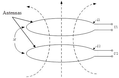
This figure shows the principles of high-frequency (HF) radio frequency identification (RFID) used in the sensing system. There is a circle labeled L1. The right side of the circle is left open, and there are two lines extending parallel from it labeled U1. There is another circle below the top one that is the exact same except with the labels L2 and U2. There is an arrow pointing at each circle labeled M. There are three dashed lines that enter through the bottom circle and exit through the top circle.
Figure 39. Illustration. Principle of HF RFID used in the sensing system.


This figure shows the equivalent circuit model for the radio frequency identification (RFID) system and the load modulation scheme for wireless communication. In this figure, a circuit is shown. The input port, U0, is connected to the capacitor C1, resistor R1, and an inductor L1. The inductor, L1, is coupled with another inductor, L2, with a coupling coefficient of M. Going clockwise from L2 is a resistor R2 in series. The output port U2 is connected to a capacitor C2 whose one plate is connected to R2, and the other is connected to L2. Resistor RL is connected in parallel with C2, and a switch labeled S and resistor labeled RM is connected in parallel with it.
Figure 40. Illustration. Equivalent circuit model for the RFID system and the load modulation scheme for wireless communication.


U times 0 equals R subscript 1 times i subscript 1 plus omega squared times M squared divided by R subscript 2 plus j times omega times L subscript 2 plus C subscript 2 times R subscript z all multiplied by i subscript 1.
Figure 41. Equation. Input voltage.


Where:
i1 = Current in the reader resonance circuit.
ω = Resonance frequency.
RZ = Load resistance.

In the case of ohmic load modulation, a switch, S, is used to change the load resistance of the sensor. Two possible resistance values can be attached to the load, resistor RL (see figure 40), and resistors RL||RM (see figure 40). These two states are used for amplitude shift key (ASK) modulation between the reader and sensor for wireless communication.

3.2 CIRCUIT IMPLEMENTATION

The ASK modulation is achieved with a single NMOS transistor whose gate is connected to the data output of the sensor. In the design, the data are in a serial pattern from the ADC, which samples the source voltage of each FG channel. When data = 0, the NMOS transistor is turned off, and the resistor seen by the reader is Rsensor. When data = 1, the NMOS is turned on and the load resistor becomes 0. The different values of the resistor will change the amplitude of the RF signal. The design of the reader, shown in figure 42, is based on the TRF7960 chip from TI. TRF7960 is a fully integrated 13.56-MHz RFID front-end and data framing reader system. The 13.56-MHz crystal generates the local clock signal for the RF front end. The reader system can transmit the RF signal through the coil to the sensor and sense the variation of the envelope from the sensor part. The reader system is controlled by the field-programmable gate array (FPGA) for setting commands or receiving data.

This illustration shows the system-level architecture of the wireless communication system for the sensor. There are two lines going from the sensor-one leads to a node and the other leads to a line labeled data. The line at the node splits; one wire goes to an antenna and the other wire goes to the drain of an N-type metal oxide semiconductor. The source is grounded. The gate is connected to the data output from the sensor block. Next to this, there is an antenna that is aligned with the other. From this antenna, a line leads to a Z-matching circuit. Next, there is a line leading to another box labeled Tx_out and Rx_AM/PM. There are another set of lines leaving this box with arrows back to the Z-matching circuit. Below the Tx_out and Rx_AM/PM box, there is a smaller block marked 13.56 MHz crystal. Two lines connect the two, one going in and the other out. To the right of the Tx_out and Rx_AM/PM box, there is another box labeled field-programmable gate array (FPGA). There are two lines connecting the two with oppositely pointing arrows, and this region is labeled data clock.
Figure 42. Illustration. System-level architecture of the wireless communication system for the sensor.


The system architecture of the sensor is shown in figure 43, and the micrograph of a CMOS prototype sensor is shown in figure 44. The core component of the sensor is the FG analog processor, which is self-powered by the piezoelectric transducer.

The communication module in figure 44 consists of: (a) ADC, (b) voltage multiplier, (c) demodulator and backscatter modulator, (d) high-voltage generator, and (e) digital base-band module (DBM).
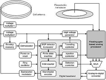
This figure shows is a flowchart of the system architecture of the sensor. It begins in the upper left corner with a coil antenna, which leads to a voltage multiplier 1, voltage multiplier 2, envelope recover, and backscatter modulator. From the voltage multiplier 1, there is a line leading to the floating gate-based analog processor, followed by a multiplexer (MUX) and an analog-to-digital converter. The other voltage multiplier leads to a demodulator, the envelope recovery, and the high-voltage generator, which leads to the floating gate-based analog processor. From the demodulator, there is the state-of-frame (SOF) detector and decoder, which connects to the finite state machine, followed by the 8-bit counter and the Manchester encoder. It then leads back to the backscatter modulator. From the finite state machine, there are three arrows that break off, one leading to the tunneling controller then to the high-voltage generator, the second leading to an injection controller which leads to the floating gate-based analog processor, and the third leading to a selection controller and then to the MUX.
Figure 43. Illustration. Architecture of the sensor.
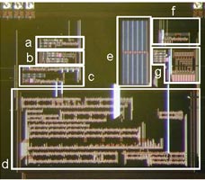
 

This photo shows a micrograph of the sensor prototyped in a 0.2-mil (0.5-micron) complementary metal oxide semiconductor (CMOS) process. There is a green box with sections labeled A through F where A is the analog-to-digital converter, B is the voltage multiplier, C is the demodulator and backscatter modulator, D is the high-voltage generator, E is the digital base-band module, F is the input circuit, and G is the floating gate circuit.
Figure 44. Photo. Micrograph of the sensor prototyped in a 0.2-mil (0.5-μm) CMOS process.


3.2.1 Envelope Recovery Circuit

The envelope recovery circuit used in the sensor is shown in figure 45. The voltage doubler implements a signal amplifier (gain equals 2), a rectifier, and a low-pass (cut-off frequency of approximately 200 KHz). Thus, the signal, V1, extracts the envelope from the received RF signal Vrf. Signal V1 is low-pass filtered by another resistor-capacitor cascade to obtain an average signal, V2. V1 and V2 are then compared using a comparator (highlighted in red), which produces a digitized version of the envelope.
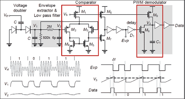
This illustration shows an envelope recovery module. There is a circuit at the top of the illustration, which begins with a connector labeled V subscript rf. It is connected in series to a capacitor, which leads to a node that breaks off into two. The left half goes to a diode and ends at the ground, and the right half continues on to another diode and then to a node labeled V subscript 1. At V subscript 1, there is a split in the wire, where half and runs into a capacitor C and then to the ground, and the other half goes to a node where the wire is split three ways. One section runs to a resistor labeled 500k and then to the ground. The second runs to a resistor labeled 2M and then to a node labeled V subscript 2, and the third connects at P-type metal oxide semiconductor (PMOS) M3. From node V subscript 2, the wire splits into two; half goes to a capacitor with the value of 6p and then to the ground, and the other goes to PMOS M2. The source of M2 is connected to the source of M3 and to the drain of PMOS M1. The drain of M2 is connected N-type metal oxide semiconductor (NMOS) M4 whose source is grounded and the gate and drain shorted. Between M5 and M3, there is a node with a wire extending to the gate of NMOS M7. The source of M7 goes to the ground, and the drain goes to a node where the wire splits. One side extends to drain of PMOS M6, and one side goes to two inverters in series followed by a node where the wire splits. Half goes to Evp and ends, and the other half goes to inverter D1 where it is labeled delay. The sources of M1 and M6 go to the supply. From D1, the wire goes to the gate of NMOS M8 where the source goes to the ground, and the drain goes to a node labeled V subscript 3. At V subscript 3, the wire splits three ways: one wire goes to capacitor C subscript 1 then to the ground, the second wire goes to two inverters connected in series and ends at a connector labeled data, and the last wire goes to the drain of PMOS M9. Gates for M1, M6, and M9 are connected together to a node labeled V subscript b. Below the circuit, three waveforms are shown. The first represents V subscript rf. The line shows five large peaks followed by three smaller peaks under the section labeled 1. Next, there are two large peaks followed by three smaller peaks under a section labeled 0. This signal is an amplitude shift key modulated wave and is sending binary codes 1,0,1,1. The next line represents V subscript 1 and has a sharp increase that flattens out before quickly decreasing under the section labeled 1. Next, there is a sharp increase that quickly flattens and then quickly decreases under a section labeled 0. The graph then repeats section 1 two more times before ending. V subscript 1 extracts the envelope from V subscript rf. The next line represents V subscript 2. It is almost completely horizontal aside from small, long bumps under section 1 and small, short bumps under section 0. Similar the other two graphs, it repeats the pattern of section 1,0,1,1. V subscript 2 is the average of V subscript 1. Next to these three graphs, there are three more graphs: Evp, V subscript 3, and data. Evp is the pulse interval encoding (PIE) comment that V subscript rf was carrying. V subscript 3 shows the charging of the node according to the length of 1 in Evp. Data becomes 1 whenever V subscript 3 crosses the threshold.
Figure 45. Illustration. Envelope recovery module.


Figure 46 shows a simulation experiment where a 13.56-MHz RF signal was induced across the sensor antenna. The envelope of the RF signal is modulated by a random noise process. However, the comparator in previous versions of the sensor does not differentiate between envelope variations caused by ambient noise and envelope variations due to ASK modulation.

As a result, the compared recovers an envelope that matches the preamble and a valid command. This forces the state machine on the sensor to randomly switch states. In the newer version of the sensor, the problem was rectified by using a hysteretic comparator (see figure 47).
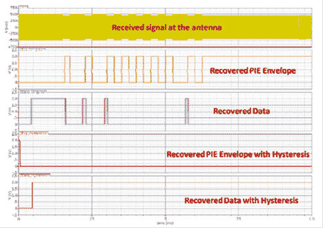
The graph shows the output of the envelope recovery module using hysteretic and non-hysteretic comparators when a noise radio frequency (RF) signal is applied. The graph is divided into five layers, from top to bottom: received signal at the antenna, recovered PIE envelope, recovered data, recovered PIE envelope and hysteresis, and recovered data with hysteresis. The x-axis shows time in milliseconds, and the y-axis is volts. The bottom portion of the graph shows the recovered data with hysteresis. The line is red and begins at 0, travels horizontally until it reaches 0.05 ms, increases straight up to 2 V, and then continues horizontally down to 1 ms. The next section shows the recovered PIE envelope with hysteresis. The line is red and beings at 2 V and instantly descends to 0 V, where it remains for the rest of the graph. The plot above this one describes the recovered data with non-hysteresis. The line is blue and begins a 0 V. Just before 0.05 ms, it increases to 2 V, continues horizontally for 0.01 ms, and then goes straight back down to 0 V. It jumps up like this three other times but only remains at 2 V for 0.0125 ms each time. The next portion of the graph describes the recovered PIE envelope without hysteria. The line is orange and begins at 2 V and descends to 0 V while still at 0 ms. It continues to 0.15 ms at 0 V, where it jumps to 2 V for about 0.025 ms and then returns down to 0 V. This pattern continues for eight cycles, and on the ninth cycle, it remains at 2 V until the end of the graph. The top portion of the graph describes the received signal at the antenna. The line is thick yellow and ranges from -500 to 500 V. It is symmetrical, and at 0.15 V, it goes to -450 to 450 V. After 0.025 ms, it returns to its original position. It repeats this pattern eight times until the last where it remains at -450 to 450 V.
Figure 46. Graph. Output of the envelope recovery module using hysteretic and non-hysteretic comparators when a noisy RF signal is applied.
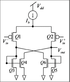
 

This figure shows a hysteretic comparator used in the improved envelope recovery circuit. The circuit begins at a supply labeled V subscript dd and goes to a current source, I subscript b. It then leads to a node where the circuit splits into two. The right side leads a source of a P-type metal oxide semiconductor (PMOS) labeled Q2, with its gate connected to V+ subscript in. The left side leads to the source of PMOSQ1 whose gate is connected to V- subscript in. The drain of Q2 is connected to V subscript out. V subscript out is connected to the drain of N-type metal oxide semiconductor (NMOS) Q4 and the drain of NMOS Q5. The drain of Q1 is connected to the drains of NMOS Q3 and Q6. The gates of Q3 and Q4 are common and are connected to the drain of Q3. Similarly, the gates of Q6 and Q5 are common and are connected to the drain of Q5. The sources of Q3, Q4, Q5, and Q6 go to the ground.
Figure 47. Illustration. Hysteretic comparator used in the improved envelope recovery circuit.


A comparator consists of cross-coupled NMOS transistors Q4 and Q5 (see figure 47), which introduce a dead zone where the comparator does not respond. The difference between the two input signals, Vin+ and Vin-, has to be greater than a certain value. Figure 46 (bottom two plots) shows the output of the envelope recovery module where the comparator does not produce any transition when the variations in RF signal envelope is small (less than 50 mV). Figure 48  shows the response of two envelope recovery modules (using conventional comparator and hysteretic comparator) for a 100 percent ASK modulated RF signal. The response shows that both modules can successfully decode the preamble and command. An additional advantage of using the hysteretic comparator is that it will reduce the output switching noise and the dynamic power dissipation of the system. Figure 49  shows the measured result obtained from the modified envelope recovery circuit (that includes the hysteresis comparator). The results show an improved demodulation performance.
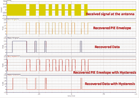
This figure shows the output of the envelope recovery module using hysteretic and non-hysteretic comparators when a valid amplitude shift key (ASK) modulated signal is applied. The graph is divided into five layers, from top to bottom: received signal at the antenna, recovered PIE envelope, recovered data, recovered PIE envelope and hysteresis, and recovered data with hysteresis. The x-axis shows time in milliseconds, and the y-axis shows volts. The bottom portion of the graph shows the recovered data with hysteresis. The line is red and begins at 0, travels horizontally until it reaches 0.05 ms, jumps straight up to 2 V, and then continues horizontally to 0.15 ms, where it then descends to 0 V. It remains at 0 V until 0.225 ms and then jumps back up to 2 V for 0.0125 ms before returning to 0 V. It makes this small jump two more times at 0.3 ms and at 0.575 ms. The next section shows the recovered PIE envelope with hysteresis. The line is red and begins at 2 V and instantly descends to 0 V, where it remains until 0.15 ms. It then jumps to 2 V for 0.125 ms before returning to 0 V. It repeats this eight times. The ninth time, it remains at 2 V. The plot above this one describes the recovered data with non-hysteresis. The line is blue and begins at 0 V. Just before 0.05 ms, it jumps straight up to 2 V, continues horizontally for 0.01 ms, and then goes straight down to 0 V. It jumps up like this three other times but only remains at 2 V for 0.0125 ms each time. The next portion of the graph describes the recovered PIE envelope without hysteria. The line is orange and begins at 2 V and then descends to 0 V at 0 ms. It continues at 0 V to 0.15 ms when it jumps to 2 V for about 0.025 ms and then returns down to 0 V. This pattern continues for eight cycles, and then on the ninth cycle, it remains at 2 V until the end of the graph. The top portion of the graph describes the received signal at the antenna, and is it shown in yellow. The yellow line is thick and ranges from -500 to 500 V. It is symmetrical, and at 0.15 V, it goes to -100 to 100 V. After 0.025 ms, it returns to its original position. It continues this pattern eight times until the last, where it remains at -100 to 100 V.
Figure 48. Graph. Output of the envelope recovery module using hysteretic and non-hysteretic comparators when a valid ASK modulated RF signal is applied.
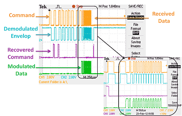
 

This illustration shows measured output of the envelope recovery module using hysteretic and non-hysteretic comparators when a valid amplitude shift key (ASK) modulated radio frequency (RF) signal is applied. Four plots are shown in this figure: command signal, the demodulated envelop, recovered command at the receiver, and modulated data. They represent the output of the envelope recovery module. A close up of the curves shows the area with the highest variation of the signals.
Figure 49. Illustration. Measured output of the envelope recovery module using hysteretic and non-hysteretic comparators when a valid ASK modulated RF signal is applied.


3.2.2 ADC

ADC selects each channel of the FG processor and encodes the stored parameter into a digital encoded data. In this prototype, there is an 8-bit single-slope ADC on the sensor. The structure of the ADC is shown in figure 50 . Before the conversion starts, S1 is zero, and the voltage on the storage capacitor Cst is charged to the input voltage Vin. When the conversion is triggered by setting S1 to 1, Cst is disconnected to the input, and a constant current source Idis begins to discharge the capacitor. Assuming the current is constant, the discharging speed of Vst is also constant. Meanwhile, the 8-bit counter is triggered by S1 and records the total discharging period from Vin to Vreg. When Vst is reduced below Vref, the output of the comparator is reserved, and the counter stops. The residential value in the counter can be expressed as the equation in figure 51.
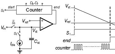
This figure shows the functional architecture of the single-slope analog-to-digital converter (ADC). There are two illustrations shown. The illustration on the left shows the structure of the ADC sensor. It begins at a connector labeled S subscript 1 with a wire labeled  start  running to a box labeled  counter.  D subscript 0 to D subscript 7 is written above the counter. The wire leaving the counter is marked  end,  and it runs to the output of an operational amplifier (OPAMP). From the positive input of the OPAMP, there is a connector, V subscript ref. From the negative input, there is a node, V subscript st. From node V subscript st, the wire splits, and half goes to capacitor C subscript st and then to a node where the wire splits. It can either go the ground or to  current source I subscript dis. From I subscript dis, the wire goes to switch S subscript 1, which is either open or closed. If it is closed, it goes a node that meets the wire or the node V subscript st . Otherwise, it goes to another switch S subscript 1 (bar), which is either open or closed. If it is closed, it goes to the connector V subscript in. The illustration on the right shows two parallel dashed lines. There is a straight line labeled V subscript ref running between them. Above that line, there is a linear line labeled V subscript st, which ends at the same point as V subscript ref. Below these lines, there is another line labeled S subscript 1, which runs parallel to V subscript ref. Below this line, there is another line labeled  end,  which also runs parallel to the others. The bottom line is labeled  counter  Starting from the left, it jumps straight up, plateaus for a second, and then goes back down. This repeats four times on the right and four times on the left and is connected through the middle by a dashed line.
Figure 50. Illustration. Functional architecture of the single-slope ADC.


n equals f subscript clk times C subscript st times open parenthesis V subscript in minus V subscript ref closed parenthesis divided by I subscript dis.
Figure 51. Equation. Residential value in the counter.


Where:
fclk = Clock frequency for the counter.

In figure 50, the bias current of the comparator is set to be 1.5 μA, which insures that the total power consumption of the ADC is low.

Improvements to the ADC were also performed by using large-size integrating capacitors and introducing a topology of a sample-and-hold circuit to reduce the effect of channel charge injection and clock feedthrough. Figure 52 shows the measured responses from the fabricated ADC when its input voltage is varied.
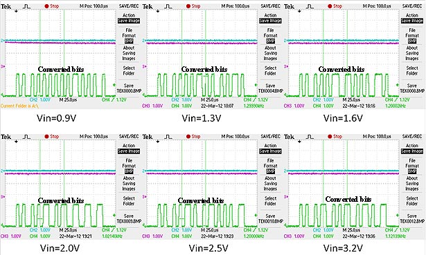
This graph shows the digital output stream produced by the analog-to-digital converter (ADC) when the input voltage is varied. The output stream is a voltage signal that alternates between high and low positions. Only the bits within the green highlighted markers represent the converted bits. Six curves are shown for different input voltages: 0.9, 1.3, 1.6, 2, 2.6, and 3.2 V.
Figure 52. Graph. Digital output stream produced by the ADC when the input voltage is varied.


3.2.3 Voltage Multiplier

In most RF power harvesting systems, the amplitude of the induced RF signal from the antenna is usually small and is not enough to operate any other circuit components. The voltage multiplier is employed to boost the weak signal to a sufficiently high level and to build charge on an on-sensor capacitor. The structure of the multiplier is based on the Dickson voltage multiplier architecture in figure 53 . Using the diodes, the current is only allowed in the direction that charges the capacitor in the next stage. For a multiple-stage voltage multiplier, the output voltage can be expressed as shown in figure 54.
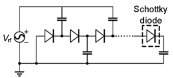
This illustration shows the structure of the Dickson voltage multiplier. It begins at the alternating current input source following the negative side and goes to a node that splits. Half goes to the ground, and the other half goes to another node, where the wire splits again. Half goes to the anode of a diode, and its cathode goes to a node that splits. One side goes to a capacitor, which is connected in parallel with the positive side of V subscript rf. The other side goes to the anode of another diode, and its cathode goes to a node which again splits. Half goes to a capacitor that is connected in series to the ground, and the other goes to the anode of another diode. The cathode of that diode goes to a node where the wire splits. Half goes to a capacitor in series with V subscript rf, and the other goes to the anode of the Schottky diode. The cathode of the Schottky diode goes to a capacitor that is connected in series to the ground.
Figure 53. Illustration. Structure of the Dickson voltage multiplier.


V subscript out equals N times open parenthesis C divided by C plus C subscript par, times V subscript rf minus V subscript on minus V subscript load closed parenthesis.
Figure 54. Equation. Output voltage.


Where:
C = Storage capacitor.
Cpar = Parasitic capacitor.
Von = Turn-on voltage for the diode.
Vload = Additional voltage drop depending on the load current.

The induced RF signal Vrf is typically less than 1 V. As a result, diodes with large turn-on voltage significantly decrease the generated voltage. The diode is usually replaced by a diode-connected transistor in the design, so a low-threshold or zero-threshold transistor is preferred for the voltage multiplier. When the low-threshold process is not available, using a Schottky diode is another option to reduce Von. A group of Schottky diodes with a different number of fingers and same junction area have been fabricated in a 0.02-mil (0.5-μm) standard CMOS process. The diode with more fingers shows smaller Von due to the reduction of the parasitic resistor. However, the reversed current will also increase for the diode with more fingers. All the turn-on voltages for Schottky diodes are measured to be close to 300 mV, which is much less than Vth for the process (0.7 for NMOS and -0.9 for PMOS).

3.2.4 Demodulator and Backscatter Modulator

The demodulator module on the sensor is used to acquire command and control information (also known as forward link) from the reader, whereas the backscatter modulator is used to modulate the impedance of the coil and establish a reverse link communication from the sensor to the reader. The system architecture implementing the demodulator and backscatter modulator is shown in figure 55. In the forward link from the reader to the sensor, a pulse width modulation (PWM) approach is used, where a pulse width of 75 ms indicates 1 and a pulse width of 50 ms indicates 0. When the reader is sending a command, the variation on the RF envelope can be detected. The recovered pulse signal itself resets the integrator and generates a different level according to the pulse width. Afterwards, a level crossing decodes the received bit. For the backward link from sensor to reader, a simple backscatter scheme is applied. After the voltage is sampled by the ADC, the result is encoded to a serial Manchester code for transmission. The transmitted data are directly applied to the gate of the backscatter NMOS transistor. The equivalent impedance seen from the antenna is changed when the NMOS transistor is turned on/off. Such difference results in a variation on the RF envelope which can be sensed by the reader.
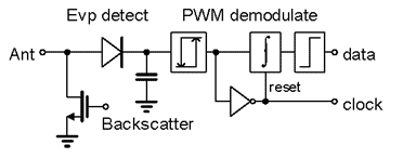
This figure shows function blocks of the modulator and demodulator. The circuit begins at an antenna, which goes to a node where the wire splits. Half goes to the drain of an N-type metal oxide semiconductor. Its gate comes from a connector, and its source goes to the ground. The other half goes to the anode of a diode. From the cathode of the diode, there is a node whose wire splits. Half goes to a capacitor and to the ground, and the other half goes to a box labeled pulse width modulation demodulate. From that box, there is a node that splits. Half goes to an inverter and to a node labeled reset, and the other goes to an integrator. From the integrator, there are two lines. One goes to the hysteric comparator and to a node labeled data, and the other goes to a node labeled reset. From the reset node, there is a line that leads to another node labeled clock.
Figure 55. Illustration. Function blocks of the modulator and demodulator.

3.2.5 High-Voltage Generator

Initializing and configuring FG transistors in the analog processor requires on-chip, high-voltage generation (> 17 V for FN tunneling and > 5 V for hot electron injection). This is challenging because the CMOS fabrication process chosen for this project supports only n-well isolation, and the rated break-down voltage of the oxide layers is approximately 8 V. Researchers implemented a high-voltage generator using a modified Dickson charge-pump architecture (see figure 56 and figure 57). Each stage of the charge pump consists of bulk-driven PMOS diodes, which are driven by non-overlapping clocks. Like a Dickson charge-pump, in each clock-cycle, charge builds up at the intermediate capacitor and the PMOS circuit provides bulk isolation from other on-chip supply voltages. Thus, the proposed charge pump can generate voltages as high as 20 V. This has been verified using measurement results from a fabricated prototype, and a sample result is shown in figure 58. The generated voltage has a monotonic relationship with respect to the frequency of the non-overlapping clocks because higher the frequency the faster charge can be transferred between stages of the charge pump.
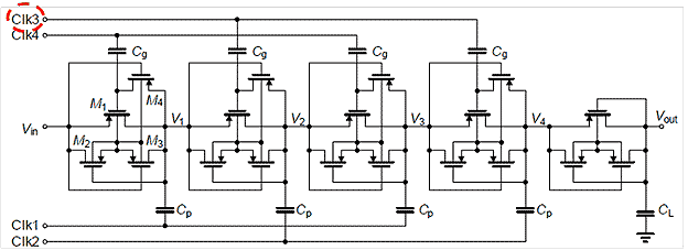
This illustration shows the charge pump used for implementing the high-voltage generator. The circuit begins at a node labeled V subscript in. This is connected to a node where the circuit splits three ways. One goes to the drain of P-type metal oxide semiconductor (PMOS) M2, another goes to the source of PMOS M1, and the third goes to the gate of PMOS M4. The gate of M1 goes to the capacitor C subscript g and the drain of M4. The drain of M1 goes to V1. The gate of M2 comes from the capacitor C subscript p, and the source for M2 and M3 comes from the gate of M1. The drain of M3 goes to both V1 and the capacitor C subscript p. C subscript p is connected to Clk1, and C subscript g is connected to Clk4. This entire section of circuit is repeated three times connected by V1-V4. The second set of capacitors goes to Clk 1 and 2 from the C subscript p side and Clk 3 and 4 from the C subscript g side. The third set of capacitors goes to the same as the first, and the last set go to only Clk 2 and Clk 3. Continuing from V4, there is another circuit of three PMOS, a connector V subscript out, and a capacitor C subscript L that leads to the ground.
Figure 56. Illustration. Charge pump used for implementing the high-voltage generator.


This illustration shows a timing diagram of the non-overlapping clock generator that drives the charge pump. There are four lines-Clk 1 through Clk 4. Clk 4 increases first, then Clk 2 decreases, then Clk 1 increases, and then Clk 3 decreases. After a period of remaining at their new positions, Clk 3 increases, then Clk 1 decreases, then Clk 2 increases, and then Clk 4 decreases. These two cycles repeat three times.
Figure 57. Illustration. Timing diagram of the non-overlapping clock generator.
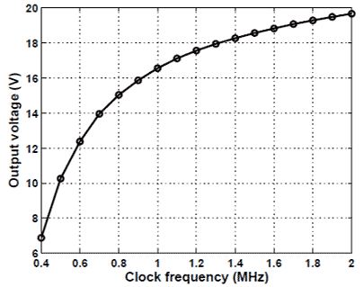
 

This graph shows sample results from a fabricated prototype. The x-axis represents clock frequency, and the y-axis represents the output voltage. The line begins at 7 V and 0.4 MHz and increases to 19.5 V at 2 MHz. The measured results illustrate that the high-voltage generator can generate up to 20 V, and the generated voltage is a function of the frequency of the non-overlapping clocks.
Figure 58. Graph. Sample results from fabricated prototype.


3.2.6 DBM

The DBM decodes the commands received from the reader and implements a state machine, which controls the configuration, initialization, and communication functions of the sensor. The functional architecture of the DBM and the state machine implemented by the DBM is shown in figure 59.
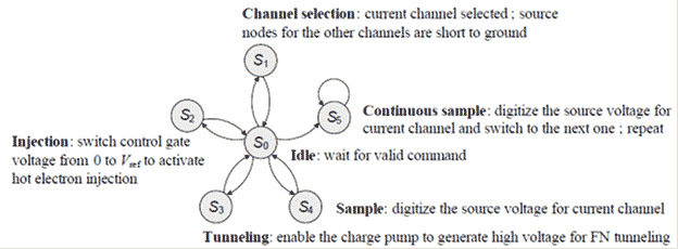
This figure shows a state machine implemented by a digital base-band module (DBM). S subscript 0 is in the center, and S subscript 1 through S subscript 5 subscript surround it in a counterclockwise direction. S subscript 1 through S subscript 4 all have arrows pointing to and from them to S subscript 0, while S subscript 5 has an arrow pointing to it from S subscript 0 and the other arrow coming out and them back towards itself.
Figure 59. Illustration. State machine implemented by DBM.


The state machine is implemented with standard CMOS logic, and the architecture has been synthesized using the standard logic synthesis procedure. By default, the state machine is in its ideal state, S0. Transition to the other states (S1S5) occurs when a valid command is received from the reader. The validity of the command is confirmed when the data packet transmitted from the reader is Manchester encoded and satisfies the parity check condition.

3.3 TESTING PROCEDURES AND MEASURED RESULTS

Prototype sensor ICs have been fabricated in a 0.02-mil (0.5-μm) standard CMOS process. The total area of the sensor IC is 0.06 × 0.06 inches (1.52 × 1.52 mm), which was then integrated on a custom-made printed circuit board (PCB) as shown in figure 60. In order to optimize the power transfer and increase the reading distance, an external reader was designed and manufactured (see figure 60). The design is based on a commercial chip TRF7960 from TI, which is a fully integrated 13.56-MHz RFID analog front-end system. The TI chip is controlled by an FPGA that has been programmed for data encoding and decoding. The reader interfaces with an embedded antenna, which fits the exact H-shape of the designed package, thus establishing a link for data transfer (the embedded antenna is shown in figure 61). The antenna is connected to the board shown in figure 60 along with the external reader to illustrate the size difference. Laboratory testing showed that the reading distance highly depends on the parasitic capacitances of the antennas and the manufactured sensor, varying between 1 and 13 inches (25.4 and 330.2 mm). These capacitances are manufacturing process dependent. As a result, individual calibration is required as well as testing under field conditions in order to assess the exact performance.
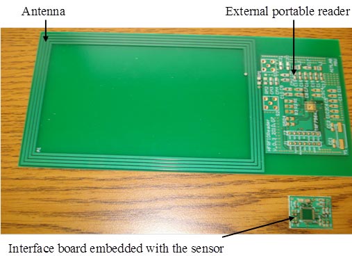
This photo shows a manufactured external reader and internal interface board. The large manufactured external reader is green, rectangular, and is divided into two parts. The left part has a plan that is outlined by four strips around the edge. The other half has an external portable reader, which looks like a microchip. The internal interface board is much smaller, green, and looks like the right half of the external reader except that it has a dark green square to the left of the center.
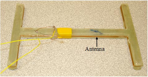
Figure 60. Photo. Manufactured external reader and internal interface board.


This photo shows a second prototype antenna adapted to the H-shaped gauge. It is yellow and in the shape of a horizontally stretched H. In the center, there is a yellow band that has two yellow strings extending from it.
Figure 61. Photo. Second prototype antenna adapted to the H-shaped gauge.


For the evaluation, the protocol processing block in TRF7960 was disabled, and another FPGA development board (SPARTAN®-3) was designed as the digital transceiver for the reader. TRF7960 was working under direct mode where the PWM data were modulated onto the 13.56-MHz RF carrier with 100 percent ASK modulation. The received data from the sensor can be detected and recovered into digital form after noise filtering and digitizing. Figure 62 and figure 63 show measured results for the ASK modulation. In figure 62, channel 2 is the sample output from ADC. It consists of the valid preamble, 8-bit data, and a 3-bit cyclic redundancy check (CRC). The data are encoded to Manchester code for transmission. Channel 3 represents the envelope variation of the RF signal. When the data equal 1 (binary code), the amplitude of the RF signal is close to 0 since the NMOS transistor shorts the load resistor to ground. When the data are 0, the amplitude of the RF signal is high. Figure 63 shows a close-up image of figure 62.

Under matching conditions, the transmitted output power from the reader is 200 mW (23 dBm) when referred to a 50-ohm load at 5 V. In the measurement, the sensor used the same coil antenna as the reader, and it was measured to be powered by the RF signal at a distance of 16 inches (406.4 mm). All the function of the control logic has been verified in interrogating mode. As shown in figure 64 and figure 65, the transition between the readout and injection state is presented according to the state machine in figure 59. As shown in figure 61, before the command to inject the FG channel is sent, the channel was within the 2–3 V range. After the injection command was recovered by the RF front end, the channel voltage increased beyond 4 V for hot electron injection. Figure 65 shows a sample result where the on-chip high-voltage generator is activated after a tunneling command is received by the sensor. The result shows that the output voltage increases to about 15 V within 625 ms. Note that a 10-M load resistance was connected at the output of the charge pump, which indicates that the open-load voltage is significantly higher and sufficient for tunneling.
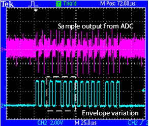
This illustration shows measured results for amplitude shift factor (ASK) modulation. The figure shows a box with two lines, the sample output from analog-to-digital converter (ACD) and the envelope variation. The sample output from ADC line begins as a thick line. It jumps up and down rapidly almost until the end, where it becomes a thick line again. The second line, the envelope variation, begins as a straight line and then jumps up vertically and flattens out for only a second before decreasing back down vertically. It repeats this 14 times and then ends as a horizontal line.
Figure 62. Illustration. Measured results for ASK modulation.
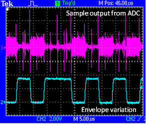
 

This illustration shows measured results for amplitude shift factor (ASK) modulation. A box is shown with two lines in it, the sample output from the analog-to-digital converter and the envelope variation. The first line has sections where the line is thick followed by portions where the line makes large jumps up and down. The sections of thick lines followed by high-jumping lines are repeated throughout the graph. Below this is the second line, the envelope variation. It begins as a horizontal line that jumps upward to a horizontal section before decreasing back down to another horizontal line. This is repeated four times.
Figure 63. Illustration. Close-up view of measured results for ASK modulation.
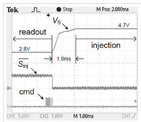
 

This figure shows the measured results showing that the sensor enters into an injection state after it receives an injection command from the reader. When V subscript s is 2.8 V, it is in the readout phase, and when V subscript s is 4.7 V, it is in the injection phase. There is a command signal (cmd) when S subscript inj goes to 0 V. V subscript s increases from 2.8 to 4.7 V with an increase in time of 1.9 ms.
Figure 64. Illustration. Measured results showing the sensor entering into an injection state.
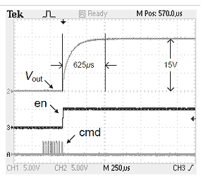
 

This figure shows the measured results showing that the sensor enters into a tunneling state after it receives a tunnel command from the reader. V subscript out begins as a straight line. Once the en line jumps to 1, V subscript out increases to 15 V. The time it takes to reach 15 V is 625 ms. The line representing cmd begins horizontally. It jumps to 1 just before the en line. The cmd line ends once the en line is at 1.
Figure 65. Illustration. Measured results showing the sensor entering into a tunnel state.


Figure 66 shows a sample result where the command was sent from the reader to remotely acquire the magnitude of the voltage stored on a FG injector channel. After the integration time required by the ADC, the 8-bit digitized result was packetized with valid preamble and 1-bit CRC code. The data packet was then communicated from the sensor to the reader using backscatter modulation using a series Manchester code. Figure 67 shows a sample result where the data on the sensor are continuously sampled (when the sensor is in state S5). As a result, the data stored in all the FG channels are digitized and backscattered to the reader sequentially.
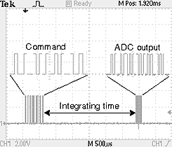
This illustration shows the results the sensor data received by the reader when it sends an acquire command. The command is on the left, and the analog-to-digital converter (ADC) output is on the right. The difference between the two is labeled the integrating time. The results of the command are spread out, while the results of the ADC output are very close together.
Figure 66. Illustration. Measured results showing the sensor data received by the reader when it sends an acquire command.
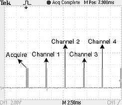
 

This illustration is the result of the multi-channel sensor data received by the reader when the sensor is in a continuous sampling state. The bar labeled  acquire  is the thickest, the bars labeled channels 1 and 3 are the second thickest, and the bars labeled channels 2 and 4 are the thinnest.
Figure 67. Illustration. Measured results showing multi-channel sensor data received by the reader when the sensor is in a continuous sampling state.


3.3.1 Testing RF Signal Propagation through Concrete and Asphalt

To test the communication protocol at the selected frequency, a set of preliminary tests were conducted. Signals were sent through concrete and asphalt (see figure 68 through figure 72). The digital command sent from the reader to the sensor was received in both cases. The feedback signal sent back from the sensor was completely recovered when transmitted in concrete (see figure 73), but it presented a loss of information when sent in asphalt (see figure 74). The thickness of the concrete slab does not affect the accuracy of the recovered signal, while asphalt introduces a reading error due to its viscoelastic properties. The energy is dissipated in asphalt more than in concrete. This issue is solved by increasing the transmitted energy from the reader.
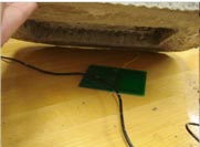
This photo shows a sensor placed under a concrete specimen.
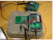
Figure 68. Photo. Sensor placed under a concrete specimen.


This photo shows a receiver placed on top of a concrete specimen.
Figure 69. Photo. Receiver placed on top of the concrete specimen.
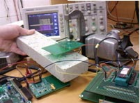
 

This photo shows a concrete specimen placed between the reader and receiver.
Figure 70. Photo. Concrete specimen placed between a reader and receiver.
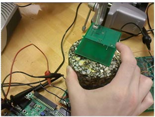
 

This photo depicts the test setup for an asphalt concrete (AC) specimen. It shows the concrete specimen with the receiver placed on top.
Figure 71. Photo. Test setup with an asphalt concrete (AC) specimen introduced between the reader and the receiver.
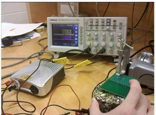
 

This photo shows the same specimen from figure 71 with wires leading from the receiver to the reader.
Figure 72. Photo. Oscilloscope showing the voltage measured at the receiver.
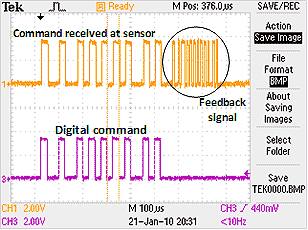
 

This figure shows the communication signal transmitted through concrete. It is divided into two parts. The top part shows the command received at the sensor. There are nine peaks followed by several very close peaks that are labeled as the  feedback signal.  Underneath is the digital command. There are nine peaks and no feedback signal.
Figure 73. Illustration. Communication signals transmitted through concrete.
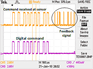
 

This figure shows the communication signals transmitted through asphalt. The upper portion shows the command received at sensor. The results are the same as figure 73 except the feedback signal is more spaced out and has fewer peaks. The bottom portion shows the digital command, which is the same as the digital command from figure 73.
Figure 74. Illustration. Communication signals transmitted through asphalt.


3.4 CHALLENGES AND IMPLEMENTED SOLUTIONS

As anticipated, the system integration of the sensor and the wireless communication protocol was one of the most challenging tasks in this study. Given the unique nature of the sensing system and based on analog FGs, an adapted and equally unique wireless protocol was completely designed and tested.

A major glitch in the high-voltage generation module caused delays, given that several versions had to be manufactured and tested. The CMOS fabrication process used for this project supports only n-well isolation, and the rated break-down voltage of the oxide layers is approximately 8 V, preventing the generation of the 18 V required for the initialization of the memory gates. After several iterations, a successful design was achieved (details are described in section 3.2.4).

As shown in figure 60 and figure 61, specific antennas were designed and manufactured for this particular system (commercially available antennas and readers cannot be used because of the low power levels at which the sensor operates). The reading distance from the sensor depends on the tuning of the wireless links for maximum power transfer, which depends on the parasitic capacitances of the antennas (embedded antenna and external reader) as well as the parasitic capacitance at the sensors' input. These capacitances are induced by the manufacturing process. The reading distance at which the system can operate (and thus the installation strategy) depends on the tuning outcome under specific field conditions.

3.4.1 RF Matching Network

Some research focused on optimizing the matching network that can maximize the read and powering distance to the sensor. The design flow is summarized in figure 75, where Rs, RL, and CL denote the reader impedance, sensor load resistance, and sensor load capacitance, respectively. Q_reader and Q_tag denote the quality (Q)-factor of the reader and the sensor, which, in-turn, determines the sensitivity of the reader. Vr, Ir, Vt, It, PRs, and PRL denote the internal electrical variables (voltage, current, and power) at the reader and sensor based on the antenna dimensions, structure, and material properties including the propagation properties of the ambient environment.
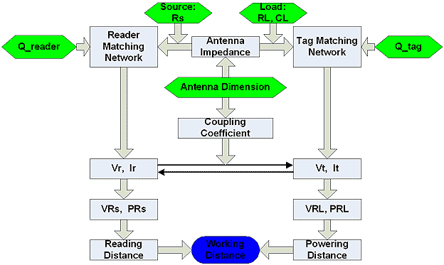
This figure shows a flowchart of the design flow to optimize the matching network that can minimize the powering and reading distance between the sensor and the reader. A box labeled  Antenna Impedance  is in the center with two arrows, one pointing to the right the other pointing the left. The arrow to the right has another arrow coming into it labeled  Load: RL, CL.  The arrows then lead to  Tag Matching Network.  Another arrow also points to  Tag Matching Network  and is labeled  Q_tag.  From  Tag Matching Network,  an arrow leads to  Vt, It  and then to  VRL, PRL.  From there, an arrow leads to  Powering Distance  and then to a blue oval labeled  Working Distance. Following the arrow to the left of  Antenna Impedance,  the arrow has another arrow coming into it labeled  Source: Rs.  The arrow then leads to  Reader Matching Network.  Another arrow also points to  Reader Matching Network  and is labeled  Q_reader.  From  Reader Matching Network,  an arrow leads to  Vr, Ir  and then to  VRs, PRs.  From there, there is an arrow leading to  Reading Distance,  which then leads to the blue oval labeled  Working Distance.  Also from  Antenna Impedance,  there is an arrow pointing at it from a box labeled  Antenna Dimension.  There is another arrow pointing from  Antenna Dimension  to  Coupling Coefficient.  From there, there is an arrow that intersects two arrows pointing in opposite directions running from  Vr, Ir  to  Vt, It.
Figure 75. Flowchart. Design flow to optimize the matching network that can maximize the powering and reading distance between the sensor and the reader.


Figure 76 and figure 77 show the sample results obtained from the design flow for a 13.56-MHz RF back-telemetry system (see figure 75). Figure 76 shows that for a 300-ohm sensor load, the maximum powering distance occurs at 8 inches (203.2 mm), whereas figure 77 shows the voltage induced at the reader when the distance between the reader and sensor is varied. These figures can be used to calibrate the electrical circuit on the sensor IC.

Researchers developed a reactive voltage-boosting technique that can be used to overcome threshold voltage limitations (and hence powering distance) imposed by voltage multipliers in an energy scavenging sensor. Experimental results have shown significant improvements in powering distance, which makes the proposed method attractive for implementing long-range inductively coupled RF sensors.
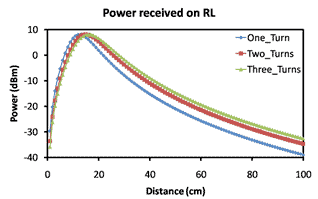
This graph shows the simulation results showing the power received at the sensor when the sensor-reader distance is varied. Distance is on the x-axis, and power is on the y-axis. There are three lines on the graph representing one turn, two turns, and three turns. All three lines originate at around -35 dBm at 0 inches (0 cm). All of the lines follow the same pattern. At a distance around 7.08 inches (18 cm), the power level is at a maximum at 9 dBm. Then, all of the lines decrease as the distance increases. At 39.37 inches (100 cm), the line for three turns is the highest at -30 dBm, followed by the line for two turns (-33 dBm). One turn is at the bottom at -40 dBM.
Figure 76. Graph. Simulation results showing the power received at the sensor when the sensor-reader distance is varied.
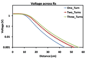
 

This graph shows the simulation results showing the voltage induced at the sensor when the sensor-reader distance is varied. Distance is on the x-axis, and voltage is on the y-axis. There are three lines on the graph representing one turn, two turns, and three turns. All three lines begin just above 1 V. They continue horizontally until 3.93 inches (10 cm) when they all begin to decrease. The line representing three turns is the highest and ends at 21.65 inches (55 cm) and 0.001 V. The next highest line is for two turns and ends around 20.47 inches (52 cm) and 0.001 V. The lowest line is for one turn and ends at 17.32 inches (44 cm) and 0.001 V.
Figure 77. Graph. Simulation results showing the voltage induced at the sensor when the sensor-reader distance is varied.


3.4.2 RF Matching Network-Voltage-Boosting Method

Several circuit techniques have been proposed to optimize the power transfer efficiency in an inductively powered sensor. However, when high throughput for data transmission between the sensor and the reader (or vice versa) is not required, then the Q-factor of the energy scavenging frontend can be traded off with the communication bandwidth according to the Bode-Fano limit. This is the case for the hybrid scavenging sensor, where mechanical events are asynchronously sensed, computed, and stored without the requirement of real-time transmission. Enhancing the Q-factor of the energy scavenging front-end has an added benefit in that it also overcomes the minimum voltage (threshold voltage) requirement for jump-starting the voltage multiplier circuits in the sensor. The efficiency of the voltage multiplying and the regulation circuit significantly improves when the input voltage is larger than the threshold voltage. Therefore, the proposed reactive voltage-boosting approach enhances the powering distance of the sensor when compared to the traditional matching techniques.

The performance of the proposed voltage-boosting method has been verified using the experimental setup shown in figure 78 in which the 13.56-MHz reader and the sensor are separated by an adjustable distance. The reader and the sensor coils have been fabricated on a planar PCB. The reader coil is driven by a TRF7960 chipset with a maximum output power set to 200 mW.

The voltage multiplier and sensor circuits are modeled by a load capacitance CL with a variable resistance RL which is inversely proportional to the power dissipation of the sensor (see figure 79). RL can also be obtained from the I-V curve in figure 80, which shows the diodic response of a typical voltage multiplier. When the input voltage VL is below the threshold voltage VON, the effective RL is large, and the multiplier is unable to boost the input voltage, resulting in ultra-low power conversion efficiency. When VL is greater than VON, RL is small enough to facilitate proper operation of the multiplier at the rated conversion efficiency. The purpose of the series matching circuit is to pre-boost VL to overcome the threshold voltage VON of the multiplier. For the proposed series matching on the transponder side (see figure 79), the sum of CP and CL should resonate with LS and CS should resonate with Lt. At 13.56 MHz, the input impedance of the sensor was measured to be CL = 72pF in parallel with RL = 200 ohm. To compare the performance of the proposed matching network, a sensor which integrates the previous parallel matching network was used as a benchmark. Therefore, for parallel matching, CP was set to 68 pF to resonant with 0.94 μH of Lt; for proposed matching, Cs was set to 140 pF, LS was chosen to be 180 nH, and CP was set to 650 pF.
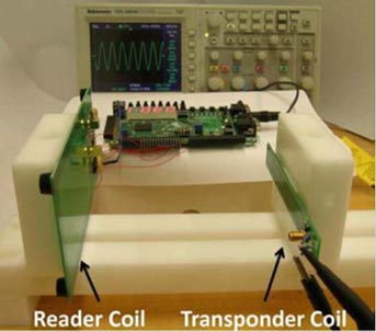
The photo shows a large horizontal plate sitting labeled the reader coil and a smaller plate parallel to the other labeled the transponder coil. There is a green electronic chip between them that is attached to each plate and to a computer.
Figure 78. Photo. Experimental setup used to validate the proposed reactive voltage-boosting method.
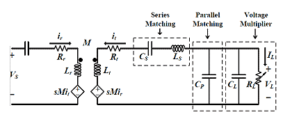
 

This illustration shows the equivalent circuit model for the setup. From the positive end of V subscript s, the circuit is connected to the resistor R subscript r, an inductor L subscript r, and a voltage source sMi subscript t. The inductor L subscript r is coupled with another inductor L subscript t with a coupling coefficient of M. Going clockwise from L subscript t is a resistor R subscript t, capacitor C subscript s, and inductor L subscript s in series. The capacitor C subscript p is connected to inducer L subscript s and to the voltage source sMi subscript r. Capacitor C subscript L is connected in parallel with C subscript p, and a resistor labeled R subscript L is connected in parallel with it.
Figure 79. Illustration. Equivalent circuit model for the setup.
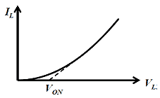
 

This graph shows the resistive model for the voltage multiplier on the sensor integrated circuit (IC). The x-axis labeled V subscript L, and the y-axis labeled I subscript L. Extending for the origin is a wide half parabola. There is a line running tangent to the parabola and intersecting the x-axis at a point labeled V subscript ON.
Figure 80. Graph. Non-linear resistive model for the voltage multiplier on the sensor IC.


The measurement results using an 18-stage loaded Schottky multiplier (for analog circuits) are shown in figure 81, where the inset shows the same response in logarithmic scale. These results show that the proposed approach can significantly boost the voltage compared to the previously used parallel matching approach. Note that the maximum output voltage of the Schottky multiplier is limited by the over-voltage protection diodes integrated on the sensor IC. Figure 82 compares the measured response obtained from a 12-stage multiplier (used for powering digital circuits). Again, the results show that the proposed matching can achieve higher output voltage.

However, compared to the results in figure 81, the improvement is not significant, which is attributed to the minimum threshold voltage required for powering the Schottky multiplier and higher load current required for driving the digital circuits.
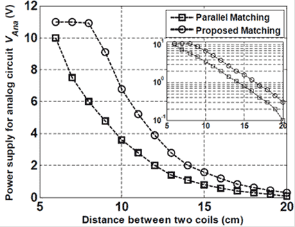
This graph shows a comparison of the voltage generated by an 18-stage voltage multiplier for the new and previously used matching network. The x-axis shows the distance between the two coils, and the y-axis shows the power supply for analog circuit V subscript Ana. There are two lines on the graph: parallel matching and proposed matching. The line for proposed matching begins at 2.36 inches (6 cm) and 11 V. It stays at 11 V until 3.15 inches (8 cm) when it decreases to 0.5 V at 7.87 inches (20 cm). The line for parallel matching begins at 2.36 inches (6 cm) at 10 V and decreases to 0 V at 7.87 inches(20 cm). There is a smaller graph in the upper right corner showing that even at 100 V, the proposed matching line is still larger than the parallel matching line.
Figure 81. Graph. Comparison of the voltage generated by an 18-stage voltage multiplier for the new and previously used matching network.
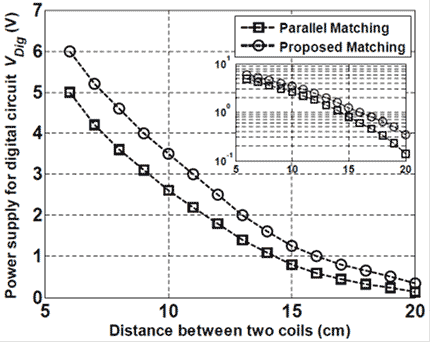
 

This graph shows a comparison of the voltage generated by a 12-stage voltage multiplier for the new and previously used matching network. The x-axis shows the distance between the two coils, and the y-axis shows the power supply for digital circuit V subscript Dig. There are two lines on the graph; parallel matching and proposed matching. The line for proposed matching begins at 2.36 inches (6 cm) and 6 V and decreases to 0.5 V at 7.87 inches (20 cm). The line for the parallel matching begins at 2.36 inches (6 cm) at 5 V and decreases to 0 V at 7.87 inches (20 cm). There is a smaller graph in the upper right corner showing that even at 100 V, the proposed matching line is still larger than the parallel matching line.
Figure 82. Graph. Comparison of the voltage generated by a 12-stage voltage multiplier for the new and previously used matching network.


3.5 CONCLUSION

This chapter describes the design and development of a novel RF communication module. The mixed mode module is specific for integration with the FG analog memories. The RF powering mode is dissociated from the computing and storage circuitry and is achieved by harvesting the RF signal. The salient modules of the RF module include the following:

In addition, an external reader was designed and manufactured. The reader interfaces with an embedded antenna, which was also designed and manufactured in-house and fits the exact H-shape of the designed package. The embedded antenna is connected to the interface. Laboratory testing showed that the reading distance highly depends on the parasitic capacitances of the antennas (embedded antenna and external reader) as well as the parasitic capacitance at the sensors input. These capacitances are induced by the manufacturing process and cannot be predicted upfront. A calibration procedure and antennas resonance tuning is required.


Federal Highway Administration | 1200 New Jersey Avenue, SE | Washington, DC 20590 | 202-366-4000
Turner-Fairbank Highway Research Center | 6300 Georgetown Pike | McLean, VA | 22101